
Graphene Transistor Design
- Alberto Ricciulli

- 8 nov 2020
- Tempo di lettura: 6 min
Aggiornamento: 10 feb 2021
In spring 2019 during my Micro-electromechanical device class me and a group of other students worked on a design project with the aim of producing a graphene transistor. This article reviews some of the scientific principles and fabrication procedures that lead us in the choices of our design. Despite the result of the ambitious project weren't successful, due to a misalignment of the mask during the fabrication procedure the project helped researcher from the MEMS lab directed by Samuel Kassagne in developing etching techniques of graphene and helped us by exposing to clean room procedures.
Graphene.
Graphene is an allotrope of Carbon whose microstructure consists of a hexagonal honeycomb monolayer of atoms. Its planar sp2 structure gives the material exceptional mechanical and electrical properties thanks to the delocalization of the electrons in the π orbital. Experimental studies show that graphene has a tensile strength of 130GPa and a Young’s modulus of 1TPa. Moreover, graphene shows a remarkable electron mobility of 200.000 cm^2/V*s which allows electrons of travelling through the material with relatively no scattering[1].
Transistor.
Transistors are electric signal controlling devices made by semiconductor materials. These constitute the most fundamental component of the integrated circuits. In most instances, transistors are composed by three electrical components: Source, Gate and Drain. Current usually flows from the source to the drain and its intensity is regulated by the gate. The path through which current flows is called channel. The channels are typically made of doped silicon. Depending on the doping element, the silicon can present an excess of electrons or electrons holes. When Silicon is doped with electron rich elements such as Phosphorus, the channel is called “n-type” and the excess negative particle act as charge carriers. On the other hand, when Silicon is doped with less electronegative atoms, such as Boron, this creates positive “holes” which are also able to conduct electricity through the material. P and n semiconductors can be utilized in pairs forming what is called a p-n junction. In a p-n junction holes and electrons will gather on opposite sides creating a depletion layer and impeding the flow of current. By applying a voltage, one can move the p or n charges and create channels through which current flows[2]–[4].
One of the most common type of transistor is the Field Effect Transistor. In FET the flow of current between the drain and the source is controlled by applying a Voltage through the gate. The Voltage generates an electric field in the device which allows for the control of the current. FETs are Unipolar devices which means they conduct through either free electron or holes, whereas other types of transistors as the BJT (Bipolar Junction Transistor) can conduct through both holes and free electrons. FETs are used in a very broad ranges of electronic applications and result very appealing thank to their smaller size compared to other types of transistors and lower power consumption. A common type of FET is the Metal Oxide Semiconductor (MOSFET). Here, the source and drain sit on heavily doped silicon of either n or p type while the channel will be doped with opposing charges. The gate sits on a metal oxide. This will allow the gate to control the current flow in the channel through the use of an electric field that filters through the metal oxide substrate[3], [4].
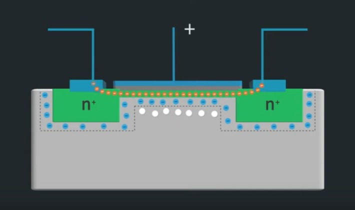
Figure 1. MOSFET Schematic. Immage from [4]
Graphene Transistor Design.
In recent years chip manufacturers have been constantly improving the designs of transistor and increasing their number in the integrated circuits by shrinking more and more their node size. Where node size is the dimension of the smaller feature in an integrated circuit. However, we are reaching a point where reducing the size further is becoming problematic as these features are already at the atomic level. Another wat to improve the processing power of integrated circuits is by replacing the features is more advanced, less conventional materials. Graphene transistors have now been a hot topic of study for many researchers thanks to the material exceptional properties. One of the applications in which graphene is currently being implemented experimentally are MOSFETs. Despite the very appealing properties such as extremely high electron mobility and very low potential dissipation, the development of this technology still presents numerous challenges. For instance, graphene does not present a band gap between the conductive band and valence band leading to problematic values voltage values to control the on/off of the current flowing through the material. Moreover, given its 2-D atomic monolayer structure, tunneling effect of atoms has to be contained to ensure the confinement of the current in the desired channel. To address such issues several designed have been proposed. A very interesting one was proposed by Fahad et al. shown in Figure 2.
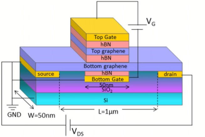
Figure 2. Graphene transistor design proposed by Fahad et al. [5]
Here, the graphene is sandwiched between layers of hexagonal Boron-Nitride (hBN). The very little lattice mismatch between Graphene and hBN and the fact that the latter do not significantly affect the electronic properties of the first makes this configuration suitable to control vertical tunneling effects of electrons. The current is regulated by adjusting the shift in the fermi level which is achieved by controlling the vertical tunneling effect in the graphene. The length and width of the graphene become crucial here. It has been experimentally observed that Graphene can conduct with no observable scattering up to a distance of a micrometer range. Moreover, such a length prevents tunneling effect between the source and drain. Width is important as it has been seen that when the length of the graphene is much larger than its width a band gap becomes observable depending on its edge type. In their study, Fahad et al. used a width of 50nm which still ensures a zero bandgap in the material [5].
Proposed Graphene-MOSFET Design.
Based on the concept previous analyzed a design shown in Figure 3 has been presented.

Figure 3. Proposed transistor design.
However, due to economical and time constraints presented during the Micro-electromechanical system design class, our design had to be readjusted to the following shown in Figure 4.

Figure 4. Schematic of fabricated graphene transistor
The expected lithographic procedure is shown in Figure 5.
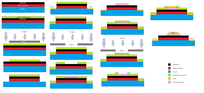
Figure 5. Lithographic procedure
Coventorware Masks are shown in Figure 6.

Figure 6. Layout of Coventorware masks
Fabrication.
Fabrication of the Graphene transistor took place in the MEMS lab and clean room directed by Dr. Samuel Kassegne. Prior to fabrication a silicon wafer was sent to Grolltex to have graphene deposited on its surface. The presence of graphene was tested through the use of a voltmeter by verifying the wafer’s surface was conductive. The wafer was then cleaned by applying three cycles of acetone, isopropyl alcohol and distilled water in sequence. Finally, the wafer was dehydrated on a hot plate to remove any moisture prior to etching processes.

Figure 7. Testing of Silicon Wafer using a Voltmeter
Shipley, a positive photoresist was utilized to protect graphene from etching (hard mask). To evenly coat with the photoresist at a desired thickness, the wafer was placed on a spin coater at 1000rpm for 45s. The wafer was then prebaked at 150°C for 90s.

Figure 8. Spin coating of photoresist
A mask aligner was used for the Graphene mask pattern with the intention to protect desired spots from UV exposure. The wafer was then exposed under a light intensity of 400mJ/cm^2. RD6 developer was successively used to remove photoresist in excess. RD6 was applied for 2 minutes. Plasma etching was then performed to remove the graphene in excess. Initial plasma etching of graphene was performed at 120W under a 200millitorr pressure for 60 seconds. This presented an issue as graphene proved to be hard to etch under such conditions. However, by increasing the power to 200W and the pressure to 600millitorr plasma etching of graphene was successful. Shipley was then washed away with acetone.

Figure 9. Plasma Etcher
The wafer was successively prepared for metal deposition by repeating the initial three cleaning cycles and by performing a 60 second plasma etch at 120W to enhance bonding of photoresist on top of the wafer. Later Futurrex negative photoresist was placed on the wafer and spin coated at 3000rpm for 10s. Wafer was then pre-baked at 150°C for 20s; exposed under a 360mJ/cm^2 light and post baked at 95°C for 300s. Developer was then applied for 7s.
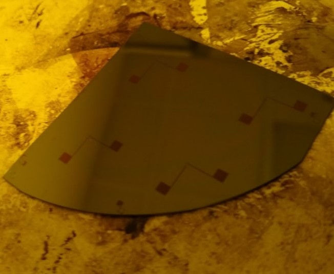
Figure 10. Wafer prepared for metal deposition of source and drain.
Chromium is used as an adhesion layer between the wafer and the source/drain. Thus, Cr metal deposition is performed prior to Gold metal deposition. Successively, cleaning and plasma etch to prepare surface are repeated as before.
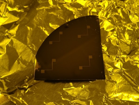
Figure 11. Wafer after metal deposition of source and drain.
For the fabrication of the Aluminum Oxide layer, Futurrex is applied and spin coated at 500rpm for 45s. The wafer is pre-baked as before, then exposed under a UV intensity of 380mJ/cm^2. Developer RD6 is then applied for 8s. Once the pattern was done, Aluminum Oxide was deposited using metal deposition. Fabrication of Gold gate pattern and metal deposition is done repeating the same steps.

Figure 12. Turbo-Pumped Sputter and Carbon Coater

Figure13. Fabricated Graphene Transistor.
References.
[1] Michael Berger, “What is Graphene,” nanowerk. [Online]. Available: https://www.nanowerk.com/what_is_graphene.php.
[2] M. Riordan, “Transistor,” Encyclopædia Britannica, 2020. [Online]. Available: https://www.britannica.com/technology/transistor/Junction-transistors.
[3] A. A. ELECTRONICS, “What is Field Effect Transistor (FET)? || Differences between BJT and FET || Types of FET.” [Online]. Available: https://www.youtube.com/watch?v=cOICDYuY-gA&t=138s.
[4] CircuitBread, “How a MOSFET Works.” [Online]. Available: https://www.youtube.com/watch?v=Bfvyj88Hs_o.
[5] M. Fahad and A. Srivastava, “A Graphene Switching Transistor for Vertical Circuit Design,” ECS J. Solid State Sci. Technol., vol. 5, no. 3, pp. M13–M21, 2016.


Commenti