
ASML Technology, A Review
- Alberto Ricciulli

- 28 set 2020
- Tempo di lettura: 7 min
Aggiornamento: 3 nov 2020
Author: Alberto Ricciulli, San Diego State University, Department of Mechanical Engineering, 2019, San Diego.
Abstract.
In 2018 ASML commercialized the NXE EUVL scanner, the first ever extreme ultraviolet scanner utilizing a 13.5nm wavelength. The implementation of such device represents a major breakthrough in the field of IC manufacturing. Huge companies such as Samsung, TSMC and Intel promptly installed this technology to further miniaturize those critical layers of nodes beyond 7nm. This review covers the scientific principles, module configuration and challenges regarding the all of the EUV subsystems.
Keywords.
ASML, EUV lithography, EUV review, EUV light source, line edge roughness, EUV mask.
1. Introduction.
Moor’s law has predicted the development and growth of the semiconductor industry over the last 50 years. A major role in keeping this improvement trend can be fairly attributed to advancements in photolithography technology. In photolithography light is used to pattern specific targets in order to create Integrated Circuits (IC)[1]. According to Rayleigh criterion, the smallest feature size achievable is given by:
Where λ is the wavelength of the used light, k1 is a process parameter known as the resolution factor and NA is the numerical aperture[2]. A larger NA will increase the wafer per hour production rate as well as the resolution however, diminishing the Depth of Focus (DOF). DOF is also important in lithography as a higher DOF allows for a reduced number of masks and cost efficiency[3].
Previous to the ASML NXE EUVL scanner, “the light source utilized in photolithography has been switching from excimer laser for i-line (365nm), to krypton fluoride (KrF) excimer laser for 248nm deep ultraviolet and to argon fluoride (ArF) for 193nm wavelength in order to get even smaller feature size”[4]. Implementation of the ArF scanner with resolution enhancement techniques and multi-patterning technologies made it possible for the industry to reach a resolution of 10nm/7nm FinFET tech node. However, to keep satisfying Moor’s law and further push the Rayleigh criterion, the industry has continuously shorten the exposure wavelength[1], [2].

Figure 1 Comparison of an ASML ArF immersion scanner and an ASML EUV scanner. Courtesy of Vu Luong, IMEC
EUVL source system is able to generate 13.5nm wavelength radiation with a maximum power of 250W (while higher power sources are currently under development). This is integrated with a fully reflective mirror system under vacuum which prevents the absorption of the EUV photons. EUV lithography system, combined with more economically suitable multi-patterning technologies can further enhance semiconductor technology node to beyond 3nm and keep Moore’s Law expectations for the next decades[2].
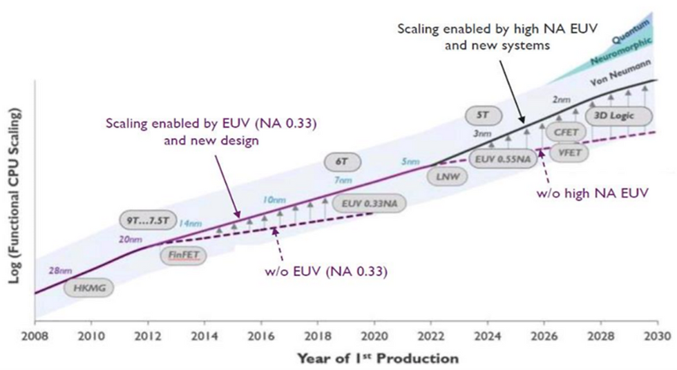
Figure 2 Technology node scaling is driven by the development of lithography and DTCO. High NA EUV will lead the industry in next decade. Courtesy of Vu Luong, IMEC.
2. Light source.
2.1. Laser Generator.
Extreme Ultraviolet (EUV) light with 13.5nm wavelength is produced by energy absorption and release of the inner electrons of a tin (Sn) particle. This is done with a high-power CO2 laser with 40-60kW by bombarding a liquid tin droplet which will cause atom ionization and generate hot dense plasma[2]. In order to achieve a high volume manufacturing (HVM), it is crucial that the wafer per hour (wph) production rate is at least of 100wph[5]. This quantity is found to be proportional to the laser power thus, a high power is demanded for the EUV source. However, such demand can’t be satisfied by the CO2 laser alone. As such, a Nd:YAG solid state laser is also used[2]. The combination of these two lasers has been nominated a “hybrid pulsed laser system”. Components of such system are: “pre-pulse seed laser, master oscillator power amplifier (MOPA), fast flow systems, beam transport system and diffusion cooled planar waveguide lasers. A system schematic is shown in Fig 3”[6].

Figure 3 Nd:YAG Laser schematic. courtesy of 2017 International Workshop on EUV Lithography , Berkeley, CA, June15th, 2017
In this setup, the first laser beam generated by the Nd:YAG Laser energizes the Sn droplet and provides the conditions by which the second CO2 laser beam is able to generate sufficient EUV to satisfy the power required for HVM. Fig. 4 illustrates the EUV generator[2].

Figure 4 "Illustration of EUV generator. Incident CO2 and Nd:YAD laser beams hit tin droplet to generate dense plasma around the droplet, with the relaxation of plasma, EUV radiation takes place and focused by the collector mirror. Courtesy of Vu Luong, IMEC."
2.2.Droplet Generator.
Internally to the EUV source subsystem, Sn droplets are continuously released with controlled size, speed and frequency from a nozzle located on top. These parameters have to be accurately calculated and evaluated at the bombard location where the laser pulse will intersect the plasma[2], [6], [7]. Studies show that the power of the EUV will depend from the droplets speed and space between the droplets. The droplet used by ASML in this application are 27μm in diameter. In this device, shown in fig. 5, an inert pressurized gas is connected to a high purity melted tin container. This container is then attached to a nozzle and the inert gas presses and regulates the flow of the melt into the nozzle[2], [6].
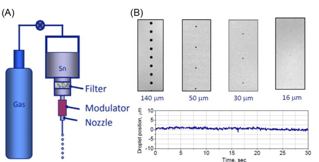
Figure 5 (A) Illustration of Sn droplet generator. (B) Snapshot of Sn droplets with different size and interval. Courtesy of Vu Luong, IMEC.
2.3.EUV Collector.
EUV photons are then collected by a highly reflective multilayer mirror (MLM). The collector is designed with a radius that enables the EUV to focus on vessel outlet named the intermediate focus (IF). From here, the EUV light is evaluated and collected into the scanner vacuum chamber[2].
Bragg’s law is utilized in the multilayer mirror to isolate and select only 13.5 EUV from the plasma halo. Here multiple layers of Mo/Si are coated on the collector and, according the bragg’s law:

, wavelength λ can be selected by variating the layer spacing and reflection angle[2], [6], [7].

Figure 6. (A) "Illustration of multilayer coated on collector mirror. (B) Photo of a real collector mirror from ASML. Courtesy of Igor Fomenkov from ASML and Vu Luong from IMEC."
The technical challenges encountered in the collector include obtaining a controlled thickness and uniformity of the mirror (MLM), avoiding degradation and oxidation of the material under EUV, surface roughness and deposition of debris and contaminants.
2.4. Power Efficiency.
It was previously mentioned that an EUV source with power of 200W at the IF is needed to reach a throughput of at least 100wph. Parameters that mostly influence the output power of the EUV source are laser power, high conversion efficiency (CE), high collection efficiency and minimization of dose overhead (losses), which gives the formula:

A 40kW CO2 laser with CE up to 6% and 10% dose overhead, are utilized in the ASML NXE3400B system, which is able to generate 250W EUV light source. Translates in a wafer throughput of around 140wph. In the meantime, ASML is currently working to develop a w400W EUV light source, which would give a 185wph production rate[2], [5], [6].
3. Reflection system.

Figure 7. Internal structure of ASML NXE:3400B scanner. Source: ASML.
13.5nm EUV are strongly adsorbed by any kind of gas. It is then necessary for the whole optical path to be fully reflective and under high vacuum. Furthermore, to reduce absorption and maximize reflectivity, a bragg mirrors system, similar to the one of the EUV collector, has been utilized. Metal based reflection mirrors are coated with alternating molybdenum and silicon (MoSi) layers with few nanometer thicknesses. In fact, the technical challenges are the same as the one of the EUV collector. Reflection optics with high NA is crucial to improve the resolution quality of the EUV scanner. Currently, a reflective system with a 0.33NA is used in the NXE3400B scanner[1], [6], [7]. However, a newly designed system of mirrors has been implemented by ASML which can provide high NA (>0.5) to boost wph and resolution. The comparison of the two mirrors are shown in fig 8[2].
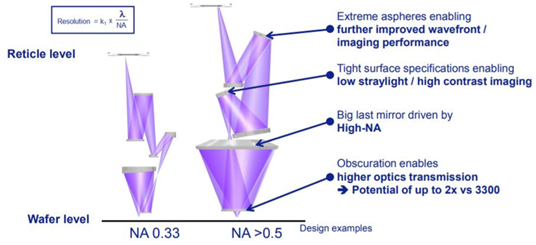
Figure 8. EUV reflection comparison between NA=0.33 and high NA mirrors. Courtesy of Anthony Yen, ASML.
4. EUV Mask & Photo Resist.
4.1. EUV Mask.
In EUV lithography having a reflective reticle on the mask is crucial for high image quality. Again, a system of Si/Mo mirrors (40 pairs) is used to get maximum reflection. These are coated by a thin film of Ruthenium (Ru) as thermal emission and reinforcing layer. On top of such layer, absorber layers will pattern the mask to form “clear” or “dark” features. Selection of the absorber material is crucial to maximize absorption and minimize reflection. EUV technology currently adopts Boron doped TaN with about 70nm thickness[1], [2], [4].
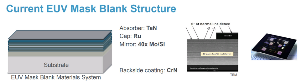
Figure 9. "EUV reticle structure illustration from Applied Materials. Courtesy of Vibhu Jindal, Applied Materials."
Mask defects represents a major challenge limiting EUV lithography HVM. Mask substrate quality is affected by its bow, surface flatness and roughness. Impurities or surface roughness can generate dislocations in the upper reticle. Is important that this is avoided as in EUV mask surface roughness of the mask may mutate the phase of the incident wave fronts which causes undesired intensity variations in the aerial image[2], [7].
4.2. EUV Photo Resist.
Compared to the deep UV lithography, line edge roughness (variations in the width of a resist feature occurring quickly along one edge) is much worse for the EUVL. This is caused by a limited light source power, short wavelength and high photon energy of EUV light, which cause stochastic effects of the photo resist. New photoresists such as metal oxide with polymer ligands are being developed and acceptable levels of LER have been reached in EUVL for HVM[2], [6].
5. Conclusions.
This paper broadly analyzes extreme ultraviolet lithography along with the challenges that this technology is facing and its application in the manufacturing of semiconductors. An overview of the main EUVL components has also been covered. Moreover, a discussion of EUV patterning performance and how this is affected by multilayer material fabrication and photoresist characteristics have also been reviewed. It’s been only in the recent years that critical obstacles have been overcome in an ASML EUV scanner system, and wafer HVM. The implementation of this technology is expected to drive chip manufacturing for the next decades and keep Moor’s law alive.
References.
[1] P. K. Krishna, M. A. Srimanth, and P. S. Reddy, “A review on contemporary practices in Lithography,” vol. 7, no. 4, pp. 27–31, 2014.
[2] N. Fu, Y. Liu, X. Ma, and Z. Chen, “EUV Lithography : State-of-the-Art Review,” vol. 19020202, pp. 1–14, 2019.
[3] L. J. Heyderman, “Paul Scherrer Institut,” vol. 8, pp. 1–10, 2009.
[4] R. Murad and H. Xichun, “Promising Lithography Techniques for Next-Generation Logic Devices,” Nanomanufacturing Metrol., vol. 9, 2018.
[5] A. Dolgov, O. Yakushev, A. Abrikosov, E. Snegirev, V. M. Krivtsun, and C. J. Lee, “Discharge-produced plasma extreme ultraviolet ( EUV ) source and ultra high vacuum chamber for studying EUV-induced processes,” pp. 1–12.
[6] I. Fomenkov, “EUV Lithography : Progress in LPP Source Power Scaling and Availability,” EUVL Work., p. P5, 2017.
[7] J. V Hermans, B. Baudemprez, G. Lorusso, E. Hendrickx, and A. Van Dijk, “Stability and imaging of the ASML EUV alpha demo tool Stability and imaging of the ASML EUV Alpha Demo Tool,” no. December 2014, 2009.
[8] R. P. Seisyan, “Nanolithography in Microelectronics : A Review,” vol. 56, no. 8, pp. 1061–1073, 2020.


Commenti